The PCB (Printed Circuit Board) plating line for high-density interconnects (HDI) represents a significant advancement in the manufacturing processes essential for modern electronics. As the demand for smaller, more efficient, and complex devices increases, so does the necessity for high-density interconnect technology, which allows for more components to be densely packed on a single substrate. This technology is critical for applications ranging from smartphones to advanced aerospace systems.
A PCB plating line specifically designed for HDI involves several key steps, each requiring specialized equipment and processes to ensure quality and precision. The first stage typically involves surface preparation, which is crucial for achieving a strong union between the conductive layers and the substrate. This stage may include chemical cleaning and micro-etching, which enhance the surface roughness, allowing for better adhesion of copper layers.
Following surface preparation, the next phase involves the application of electroless copper plating. This process can reach intricate areas, ensuring coverage even in the finest vias and microvias often found in HDI boards. The electroless plating technique creates a uniform layer that is essential for subsequent electroplating, which adds significant thickness to the copper in areas requiring increased conductivity and structural integrity.
Electroplating is a vital component of the PCB plating line where an electric current facilitates the deposition of copper onto the surface of the printed circuit board. This stage is instrumental in achieving the desired layer thickness and overall conductivity, thus supporting the intricate electrical pathways essential in high-density applications.
Quality control is paramount throughout the entire plating process. Advanced inspection technologies, including automated optical inspection (AOI) and X-ray computed tomography (CT), are employed to ensure the integrity of the plated surfaces and to identify any defects at an early stage. This attention to detail is what distinguishes a high-quality HDI PCB from standard offerings, as reliability and performance are non-negotiable in today’s electronic applications.
Moreover, the plating line's efficiency and automation play a vital role in enhancing production capacity while maintaining consistency in quality. With the shift towards smart manufacturing, many lines now incorporate real-time monitoring systems to optimize performance and reduce waste, aligning with global sustainability goals.
In summary, a PCB plating line for high-density interconnects embodies expertise in chemistry and engineering, advanced manufacturing techniques, and stringent quality control measures. By harnessing these elements, manufacturers can produce superior HDI PCBs that meet the demands of the rapidly evolving electronics landscape.

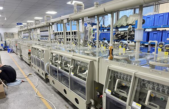
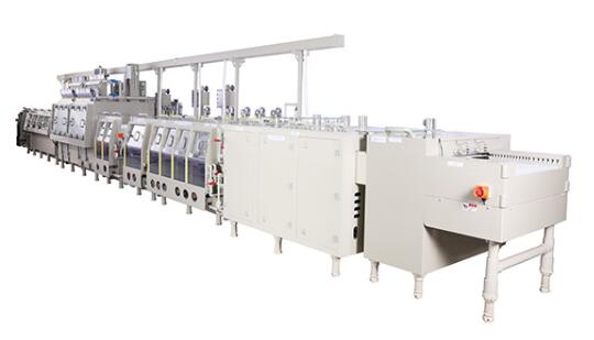
 Multi-Function PCB Plating Line