The evolution of wearable technology has brought forth a remarkable demand for innovative manufacturing processes, particularly when it comes to the production of printed circuit boards (PCBs). The PCB plating line for wearable technology represents a critical component in ensuring both the functionality and durability of these devices. In an era where the demand for miniaturization and performance optimization is ever-increasing, the plating line stands as an essential element that enhances the overall quality and reliability of PCBs used in wearables.
Wearable devices, ranging from smartwatches to health-monitoring sensors, require PCBs that can withstand the rigors of continuous use while maintaining their efficiency under a variety of conditions. The PCB plating line is designed to apply precise layers of metal onto the circuitry, ensuring excellent conductivity and protection against environmental factors like moisture and corrosion. This process involves several stages, including surface preparation, metal deposition, and finishing, each requiring specialized techniques and stringent quality control measures.
Expertly executed plating techniques, such as electroplating and immersion plating, not only ensure robust connections between components but also play a vital role in enhancing the aesthetics of wearable devices. In addition, advancements in technology have enabled the use of thinner coatings without compromising performance, aligning with the trend towards lighter and sleeker designs in wearable technology.
Experience is paramount in operating a PCB plating line, as the process demands an intricate understanding of the chemical reactions involved and the machinery used. Operators and engineers must be well-versed in the principles of electrochemistry and material science, allowing them to troubleshoot issues that may arise during production. Furthermore, today’s PCB plating lines incorporate advanced automation and data analytics, significantly improving throughput and consistency while reducing the likelihood of defects.
The authoritativeness of the PCB plating line for wearable technology stems from its pivotal role in a highly competitive market. Quality assurance standards such as IPC and ISO not only guide the manufacturing process but also ensure that the final products meet stringent safety and performance benchmarks. Manufacturers that invest in state-of-the-art PCB plating technology and adhere to these standards are better equipped to deliver durable, high-performance wearables that meet consumer expectations.
In summary, the PCB plating line for wearable technology is an indispensable aspect of modern electronics manufacturing. Its significance lies in its ability to produce reliable and efficient PCBs that form the backbone of innovative wearable devices, ultimately enhancing the user experience and driving the growth of this dynamic industry.

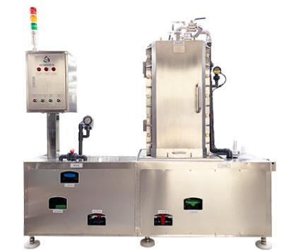
 High-Precision Semiconductor Machine